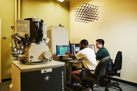
Helios NanoLab 650
The Helios NanoLab 650 features a field-emission SEM (FESEM) and focused gallium-ion beam (FIB) technologies and their combined use. As FEI’s 11th DualBeam platform, it is designed to access a new world of extreme high resolution (XHR) 2D and 3D characterization, 3D NanoPrototyping, and higher quality sample preparation.
-
High-vacuum mode
-
Non-conductive samples require conductive coating prior to imaging
-
Quantitative EDS
-
Transmission scanning electron microscopy
-
TEM foil extraction
-
3D slice-and-view for serial sectioning of samples
The Helios NanoLab™ 650 features FEI’s highly engineered advances in field emission SEM (FESEM) and focused ion beam (FIB) technologies and their combined use. It is designed to access the world of extreme high resolution (XHR) 2D and 3D characterization, 3D NanoPrototyping (Nanobuilder), and high-quality sample preparation. Robust, precise FIB slicing, combined with a high precision (150 x 150 µm) piezo stage and superb SEM performance, allows automated software for unattended sample preparation or 3D characterization and analysis (“Slice and View”). It is equipped with an OmniProbe micromanipulator for TEM sample preparation. The instrument has superb imaging capabilities, providing sub-nanometer resolution across the whole 1-30 kV range. Its through-the-lens detector sets collection efficiency of both secondary electrons (SE) and on-axis backscattered electrons (BSE), and is complemented by two multi-segment solid state detectors, a detector for backscattered electron (BSE) imaging able to detect low kV BSE, a scanning transmission electron detector able to record simultaneously bright field (BF), dark field (DF) and high angle annular dark field images (HAADF), and a third detector dedicated to FIB-SE and FIB-SI (secondary ion) imaging.
The Helios NanoLab allows focused ion beam technology and features excellent FIB imaging, outstanding low kV operation down to 500 V, and up to 65 nA beam current.
The system is equipped with a X-Max Silicon Drift Detector (SDD) EDS system by Oxford Instruments, with energy resolution of 125 eV for Mn Kα (5.899 keV). The 80 mm2 active area significantly increases the collection solid angle, which results in a detector which performs measurements either more quickly than traditional systems, or at higher resolution. The increased sensitivity allows the system to operate at much lower beam currents or low accelerating voltage, which reduces the risk of sample damage.
FEI/ThermoFisher Apreo 2S
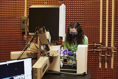
The ThermoFisher Apreo 2S (NSF MRI Award: 2018167) has high-resolution performance (1 nm) and excellent image quality at an analytical working distance (10 mm), offering worry-free operation, even for novice users. The Apreo is equipped with standard in-column detectors that can operate at a range of vacuum and voltages settings, and when combined with the EDS camera (with detection sensitivity to Be), enables both high-resolution imaging and chemical analysis on even the most challenging, uncoated, non-conductive samples. The ColorSEM uses a combination of live color imaging and conventional EDS functions allowing for quick determination of the elemental composition of the sample. The Maps 3 software is installed on both the Apreo and the Helios system allowing for automated, high-resolution imaging of large sample areas and subsequent image stitching.
The system at CWRU is equipped with additional detectors and stages that make it a unique instrument for conducting experiments under in-operando conditions.
-
The retractable cathodoluminescence (CL) detector enables the user to conduct correlative light and electron imaging for optical materials, thus correlating microstructural features with changes in material illumination.
-
The interlock kit enables the safe, reliable transfer of air-sensitive samples directly from the MORE Center glove box into the evacuated SEM chamber.
-
Lumis Electron Backscatter Diffraction (EBSD) system enables the direct collection of crystallographic orientation information from conventional samples in backscatter mode, and thin-film samples for Transmission Kikuchi Diffraction (TKD).
-
The High-Vacuum Heating Stage is used to heat samples (up to 10x10 mm2) and record in-situ morphological sample changes up to a temperature of 1100 °C with 1 °C accuracy. Fully controlled through the microscope software, it is possible to define ramp/soak profiles with a maximum recommended heating rate of 10-50°C/min. A top-down heat shield provides a large opening for live sample imaging during heating experiments, but prevents heat loss and protects sensitive detectors such as the EDS detector. An EBSD heat shield is provided for work at 70° tilt, allowing sample temperatures up to 900 °C.
-
A Hummingbird Scientific SEM liquid-cell system allows real-time imaging of solid-liquid interfaces in the SEM. The two-chip liquid cell allows users to quickly and easily prepare and exchange samples while remaining confident in the cell’s seal.


