In many cases, researchers require that they “look” at materials and devices to understand how changes in processing/environment control the microstructure. Depending on the length scale of the features of interest, different techniques are applicable for observing those features. The spatial resolution of different techniques, shown in the image below, is dependent on the wavelength of “light” being used to illuminate the sample.

Atomic force microscopy (AFM) is an interesting technique that does not require “light” to image the sample surface, and thus has different resolution constraints. This technique rasters a lever-arm that can “see” the material surface by either tapping (contacting) or sensing the electron charge (non-contacting) of the sample to measure surface height. This makes the spatial resolution limited by the rastering resolution, 1-3 microns, but the vertical resolution on the order of angstroms without the need for samples in a vacuum.
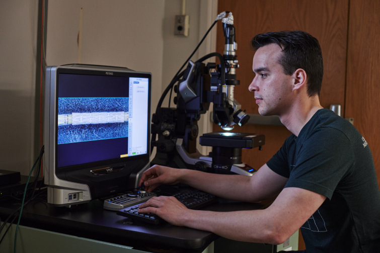
In the Swagelok Center for Surface Analysis of Materials at Case Western Reserve University, we maintain light (keyence), AFM, and electron microscopy to support the needs of researchers that need to understand microstructural features in the range of millimeters to nanometers.